

|
|
|
|
Products & Services
|
iPhone 5 Power On Time Sequence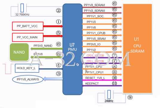 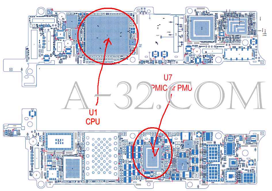 1) After a battery voltage of 3.8V inputs "PP_BATT_VCC" to U7 Pin E1, E2. (1st time voltage input to U7) 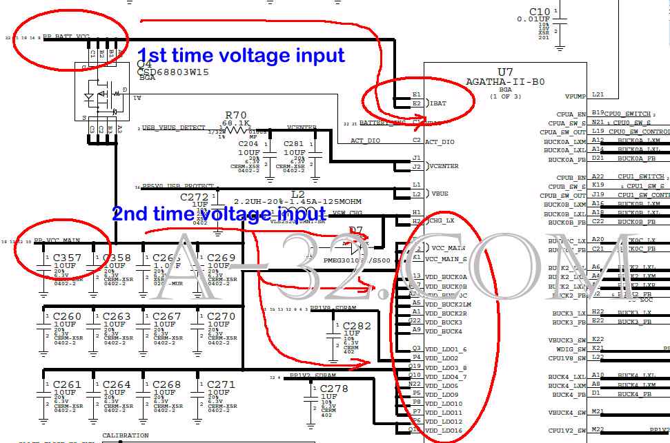 2) U7 combines with components: Y1, C276, C283 generates a clock signal of 32.768 Khz at U7 Pin P1, N1. U7 outputs a standby voltage of 1.8V "PP1V8_ALWAYS" at Pin P17. 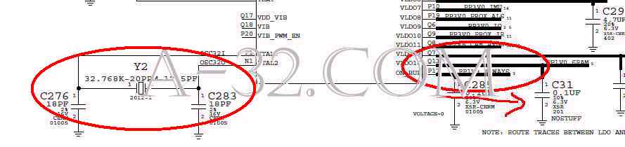 3) Press the Power button or short out DZ1 triggers a digital signal 1.8V-0V-1.8V or "HOLD_KEY_L" at J2 Pin 9 which then goes to U7 Pin K6, an output voltage of 3.8V "PP_VCC_MAIN" at U7 Pin Q15 is generated. 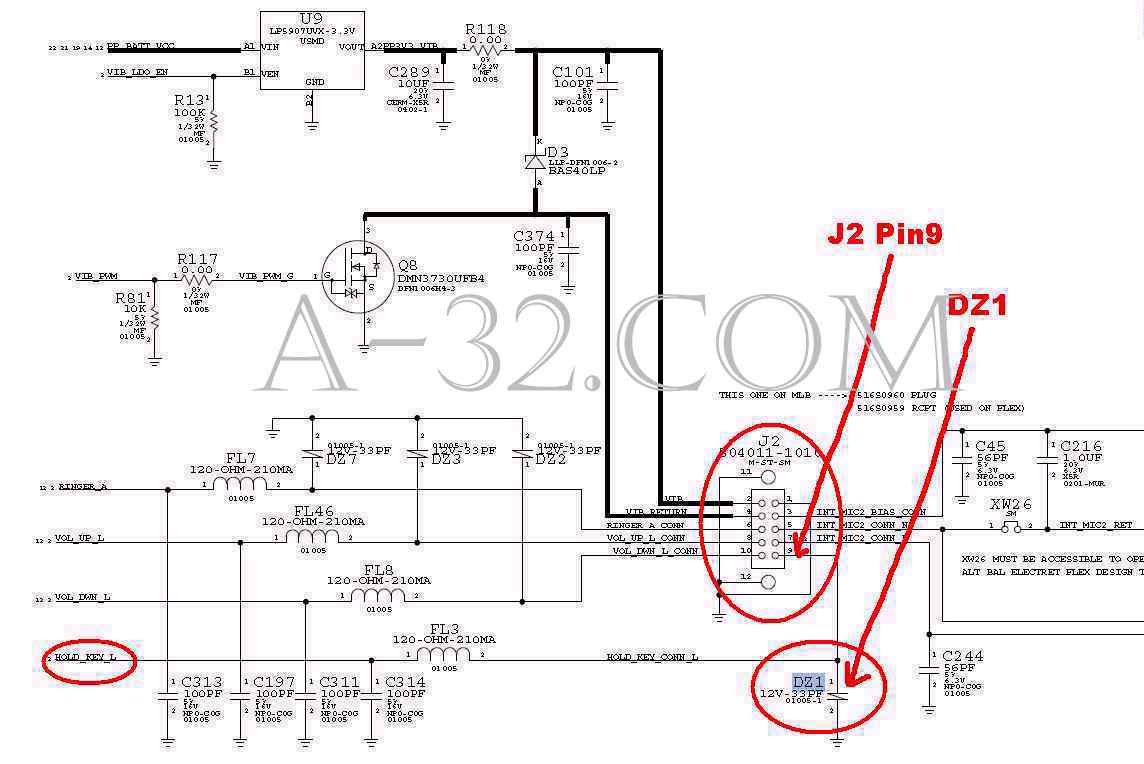 4) "VCC_MAIN" inputs to a total of 9 pins on U48's VCC_MAIN module. They are A5, A7, A10, D11, H10, G10, K5, K3, K11. (2nd time voltage input to U48)   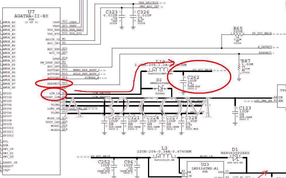 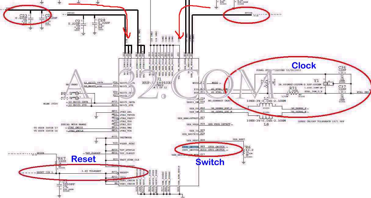 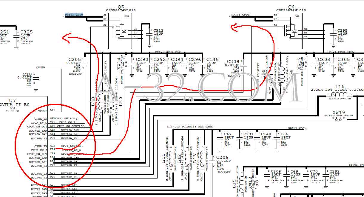 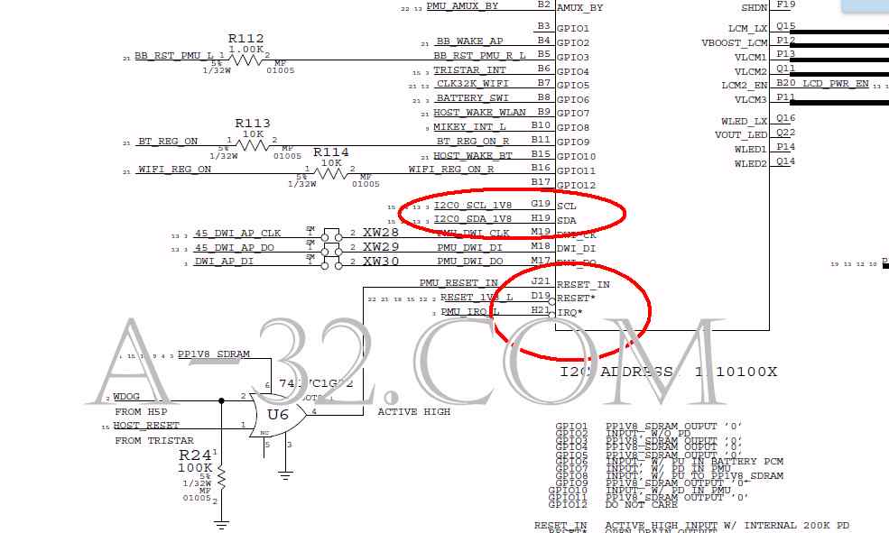 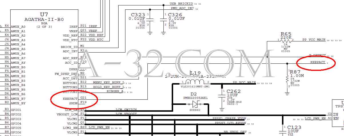  Source of all circuit diagram are from Apple's schematic. iPad, iPhone, iPod, Macbook are trademarks of Apple company. |