

|
|
|
|
Products & Services
|
iPhone 6 NO BacklightiPhone 6 LCD backlight is couple tiny LEDs. In order to light up these LEDs at the same time, a higher voltage drop is neccessary. When "PP_VCC_MAIN" goes thru circuit components L1503, D1501,C1505, C1530, and C1531 thru "PP_LCM_BL_ANODE" to LCD Panel, U1502 also powers up on pin C3. Then a chain of on-off rectangle pulses is generated on U1502 pin A3.When U1502 Pin A3 is off, energy is charged on L1503. When U1502 Pin A3 is on, energy goes thru diode D1501 then piles up on capacitors C1505 C1530, and C1531. These capacitors finally has a enough voltage drop to light up all LEDs on LCD panel at the same time. Theory on Switching Boost Circuit is shown below. NO light, NO display or dim backlight is caused by the defective of one of the component in the circuit or by defective LCD panel. Steps to troubleshoot: 1) check fuse coil L1503. If it is bad, missing or damaged, no beep or show more than 0.1 ohms, replace or jump it. 2) use voltmeter to check the continuity of diode D1501, replace if both side are short or both side are opened. 3) check if capacitors C1505 C1530, and C1531 both legs are ground or same voltage, replace if yes. 4) check IC U1502 has any damage, otherwise repalce it. 5) check circuit trace is broken or not. 6) if nothing solve above, Power IC has to replaced. 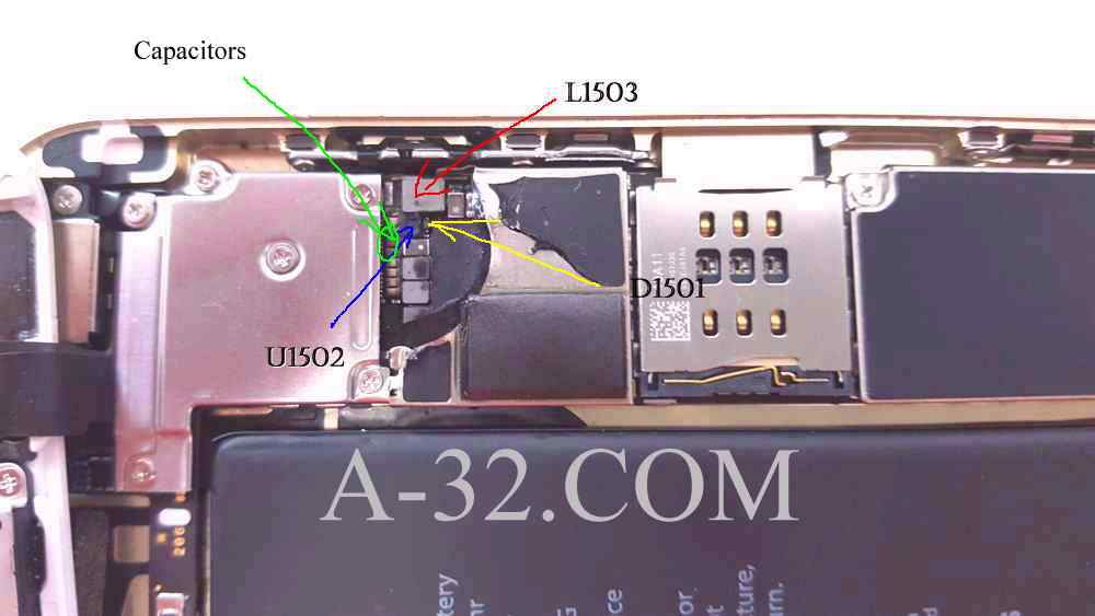 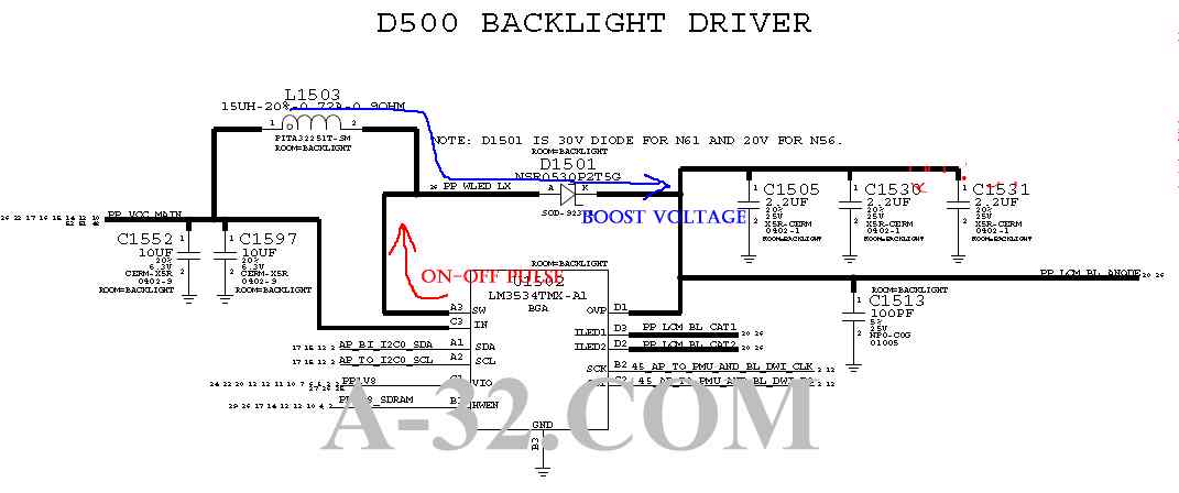 THEORY: 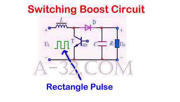 1) Switching Boost Circuit is a DC-DC converter which is by mean of ON-OFF rectangle pulse to pump up the voltage to desired level. Here is the brief illustration of this widely used circuit. As the intial pulse is HIGH, transistor turns ON to allow current go thru coil L. Coil stores eneregy in the form of magnetic field. 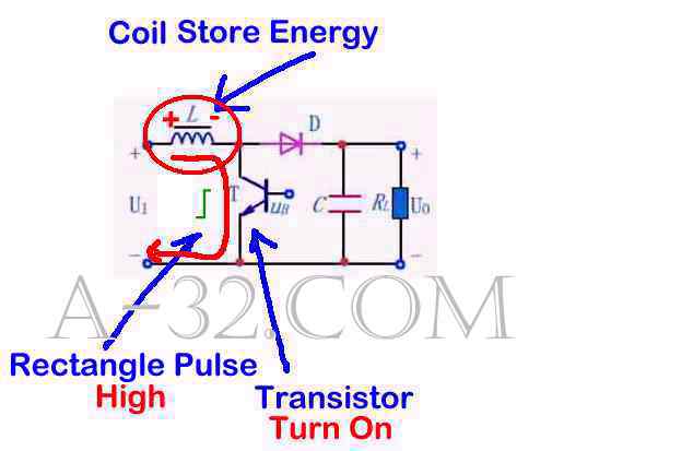 2) As the pulse goes LOW, transistor turns OFF. This sudden drop of current causes coil L to produce a back e.m.f. in the opposite polarity. This results in two voltages, the input voltage U1 and the back e.m.f.(V=VL) across L in series. Since the transistor is off, this combined voltage (U1 +VL) is no way out except that it goes thru the forward bias D and charges capacitor C. 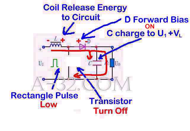 3) As the pulse goes HIGH again, transistor turns ON and L stores energy accordingly. Due to the charge on C, the cathode of D is more postive than its anode. Diode is reverse bias and then turns off. C releases a voltage of U1+VL to output (U0). 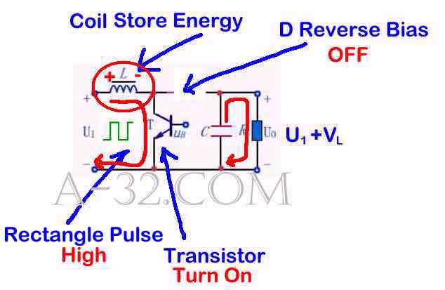 4) The output voltage (U0) is determined by the input voltage (U1) and the duty cycle (D) which is ratio between pulse HIGH (TON) and period in a rectangle pulse. For the voltage on a coil is V=L(di/dt) or di/dt=V/L. Integrate both side we have the current i=(V/L)xT where V/L is a constant for a rectangle pulse. While the transistor is ON, current at node A is ramp up, i=(U1/L)xTON. While the transistor is OFF, current at node A is ramp down i=-(U0-U1)/LxTOFF. In a steady state, total current at this node is zero, ie (U1/L)xTON + -(U0-U1)/LxTOFF = 0, simplify we have U0=U1(1+D/(1-D)), where D=duty cycle=TON/(TON+TOFF)=TON/Period For example: if duty cycle is half, ie pulse HIGH and pulse Low are equal, then output voltage will be double. U0 = 9V x (1+ 0.5/0.5) = 9V x (1+1) = 18V 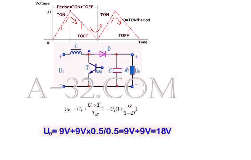 Source of all circuit diagram are from Apple's schematic. iPad, iPhone, iPod, Macbook are trademarks of Apple company. |